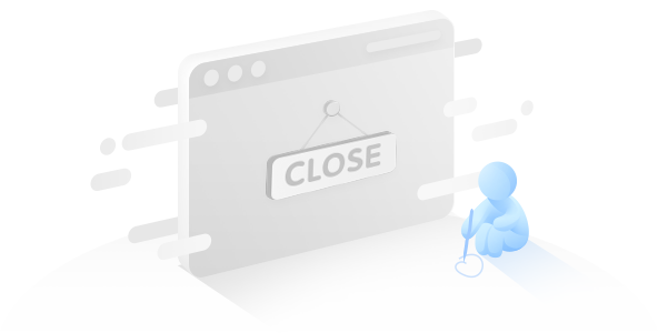
设为首页 | 收藏本站
服务热线:0755-83281126

TAITIEN(台湾泰艺)

发表时间:2018-11-21 14:18

市場應用-無線通訊網路


Quartz Crystal
Type Photo Feature Dimension
(mm)
Frequency
Range
Output Data Inq.
X3  Tight Tolerance
Ultra Low Profile
1.6 x 1.2 26~54MHz


XZ  Tight Tolerance
Compact Footprint
2.0 x 1.6 20~50MHz


X2  Full Ceramic Package
Glass Seal
3.2 x 2.5 12~48MHz


XR  Tight Tolerance6.0 x 3.5 8~49MHz


Crystal Oscillator
Type Photo Feature Dimension
(mm)
Frequency
Range
Output Data Inq.
OZ  Ultra-compact and Light
Low Jitter
Low Standby Current
2.0 x 1.6 1~50MHz CMOS

32.768kHz Series - OX/OY  Operation Voltage: 1.8V, 2.5V, 3.3V
Tri-state enable/disable
3.2 x 2.5 / 2.5 x 2.0 32.768kHz CMOS

OX-A/OY-A  Tight Stability: ±5 ppm over -40°C ~+85°C
Tight Tolerance: ±3 ppm accuracy@25°C
LVCMOS Output Logic
3.2 x 2.5 / 2.5 x 2.0 19~60MHz LVCMOS

OW-M CMOS  Very Low Phase Jitter: < 1 pS (0.6 pS, typ.) RMS Any Frequency between 10 MHz and 250 MHz Fast Delivery5.0 x 3.2 10~250MHz CMOS

OW-M LVPECL / LVDS  Very Low Phase Jitter: < 1 pS (0.6 pS, typ.) RMS Any Frequency between 10 MHz and 1500 MHz Fast Delivery5.0 x 3.2 10~1500MHz LVPECL / LVDS

OY  Smaller Size
Low Jitter
Low Standby Current
2.5 x 2.0 1~125MHz CMOS

OT-M CMOS  Very Low Phase Jitter: < 1 pS (0.6 pS, typ.) RMS Any Frequency between 10 MHz and 250 MHz Fast Delivery7.0 x 5.0 10~250MHz CMOS

OT-M LVPECL / LVDS  Very Low Phase Jitter: < 1 pS (0.6 pS, typ.) RMS Any Frequency between 10 MHz and 1500 MHz Fast Delivery7.0 x 5.0 10~1500MHz LVPECL / LVDS

OX  Low Jitter
Low Standby Current
3.2 x 2.5 1~125MHz CMOS

OW  Low JitterUp to 320MHzTri-state Enable/Disable5.0 x 3.2 80~320MHz PECL / LVDS

OV  Low Jitter
Low Standby Current
5.0 x 3.2 13.7kHz ~ 133MHz CMOS

OC  Low Jitter
Low Standby Current
7.0 x 5.0 13.7kHz ~ 166MHz CMOS

OC-M  Up To 200MHz 7.0 x 5.0 1~200MHz CMOS

OT  Low Jitter
Differential O/P
Up To 320MHz
7.0 x 5.0 19.44 ~ 320MHz PECL / LVDS

OT-U  Ultra Low Jitter
Differential Logic
7.0 x 5.0 70~170MHZ PECL

OT HCSL  Very Low Jitter
Tri-state enable/disable
Differential Logic
7.0 x 5.0 90~125MHz HCSL


VCXO
Type Photo Feature Dimension
(mm)
Frequency
Range
Output Data Inq.
VW CMOS  Smaller Size
Good Linearity
5.0 x 3.2 1.5~80MHz CMOS

VW PECL / LVDS  Smaller Size
Good Linearity
Differential Logic
5.0 x 3.2 60~175MHz PECL / LVDS

VT-A  Very Low Jitter Performance < 0.1pS RMS from 12k~20MHz Up to 800 MHz Tri-state Enable/Disable7.0 x 5.0 120~800MHz LVPECL

VT CMOS  Tight Symmetry Low Jitter   7.0 x 5.0 1.5~200MHz CMOS

VT-M CMOS  Tight Symmetry 7.0 x 5.0 60~200MHz CMOS

VT PECL / LVDS  Tight Symmetry Wide Pulling Range Low Jitter Differential Logic7.0 x 5.0 1.5~200MHz PECL / LVDS

VT-M PECL  Tight Symmetry
  Wide Pulling Range
Differential Logic Up To 800 MHz
7.0 x 5.0 100~800MHz PECL

VK  Metal Cover, FR-4 PCB Based SMD package Differential Logic Up to 200 MHz14.2 x 9.3 1.5~200MHz PECL / LVDS


VCTCXO / TCXO
Type Photo Feature Dimension
(mm)
Frequency
Range
Output Data Inq.
TV  Low Power Consumption VCTCXO Available5.0 x 3.2 10~40MHz CMOS / Clipped Sine Wave

TW  High Precision For-20°C~+ 70°C, ± 0.1 ppm-40°C~+ 85°C ± 0.28 ppm5.0 x 3.2 10~40MHz CMOS / Clipped Sine Wave

TT  High Precision For -40°C~+85°C7.0 x 5.0 5~40MHz CMOS / Clipped Sine Wave

TT Stratum3  Overall ± 4.6ppmIncluding 20 Years Aging(@ -40°C~+ 85°C)7.0 x 5.0 5~26MHz CMOS / Clipped Sine Wave

TS  High Precision For -40°C~+85°C7.0 x 5.0 5~40MHz CMOS / Clipped Sine Wave

TS Stratum3  Overall ± 4.6ppmIncluding 20 Years Aging(@ -40°C~+85°C)7.0 x 5.0 5~26MHz CMOS / Clipped Sine Wave

T9  High Precision For
-20°C~+ 70°C, ± 0.1 ppm
-40°C~+ 85°C, ± 0.28 ppm
20.4 x 12.8 10~40MHz CMOS / Clipped Sine Wave

TA  Low Power Consumption VCTCXO Available7.0 x 5.0 5~52MHz CMOS / Clipped Sine Wave

TK  Low Current Option VCTCXO Available14.3 x 8.7 5~40MHz CMOS / Clipped Sine Wave / PECL / LVDS

TF  Double Sealed VCTCXO Available20.4 x 12.8 1.25~40MHz CMOS / Clipped Sine Wave


OCXO
Type Photo Feature Dimension
(mm)
Frequency
Range
Output Data Inq.
NK-N  ±30 ppb stability over
-40 to 85°C
Low Power Consumption
Fast Warm-up
Overall ± 4.6ppm Including 20 Years Aging
14.3 x 9.3 10~40MHz CMOS

NJ

SC-CUT Crystal
High Stability
Low Phase Noise
Fast Warm-Up

25.4 x 22.1 5~40MHz CMOS /
Sine Wave


T-ESTM  Multiple Reference Signals: DCLS/1PPS
Accuracy: ≤ 50ns
1PPS + NMEA Output
DCLS Output
Overall Power Consumption Reduced to 300mW
Build-in Charge/Dischage Management Circuit
Installed with Li-Ion Battery for Wide Temperature Range
80 x 80
1PPS + NMEA,
DCLS          


分享到:
会员登录
登录
其他账号登录:
留言
回到顶部